|
Femtosecond Laser Micromachining
Femtosecond Laser Micromachining / Microfluidic Chips and Devices Manufacturing / Microfluidic / Lab-on-a-chip / Contract Manufacturing Services / Optical fibers / Space Variant Retarders / Waveplate / Wave retarder
   

Bio-Technology Raw Materials and Consumables from Taiwan
Knowledge Bases :
I. Femtosecond Laser MicromachiningUltrashort pulseMode-locking / Femtosecond laserLaser scanning / Galvanometer scannersAspect ratios
Surface roughness
Laser Marking / Laser engraving
Laser Welding
Waveguide writingMultiphoton polymerization | MPP / Multiphoton lithographyPolydimethylsiloxane (PDMS)
II. Microfluidic Chips and Devices Manufacturing / Microfluidic / Lab-on-a-chipMicrowell plates / Microplate
Point-of-care testingSingle-Cell AnalysisDroplet-based microfluidics
III. Contract Manufacturing Services
GlassTempered glassMetallic glass / Amorphous metalCeramicsSiliconSapphireMetal (Foil)
Engineering plastics / High-performance plasticsThree-dimensional integrated circuitList of integrated circuit packaging typesSpacers / Interposers
Probe Cards / Guide PlatesGuide Plates for Probe Cards
Carrier wafers / Fan-out wafer-level packagingChip carrier
IV. Optical fibersOptical fibersFibers Drilling / Tip ShapingFBG writing / Fiber Bragg grating
V. Space Variant Retarders / Waveplate / Wave retarder
WaveplatePolarization (waves)Linear polarizationS and P polarizations / Higher-order S-waveplateRadial polarizationAzimuthCircular polarizationOptical vortex / Cylindrical vector vortex
Micro-mill / Polishing / Vibratory finishingOptical tweezers / Optical trappingTransmission coefficientAR coating ( Anti-reflective coating )Laser induced damage threshold (LIDT)
Laser diode / High-power lasersCircular grating / Flat axiconGaussian beamBessel-Gauss beamFlat-Top beam / Tophat beamLaser beam profilerDepolarization compensatorActive laser medium / Gain medium
I. Femtosecond Laser Micromachining

A positively chirped ultrashort pulse of light in the time domain. |
In optics, an ultrashort pulse of light is an electromagnetic pulse whose time duration is of the order of a picosecond (10−12 second) or less. Such pulses have a broadband optical spectrum, and can be created by mode-locked oscillators.
They are commonly referred to as ultrafast events. Amplification of ultrashort pulses almost always requires the technique of chirped pulse amplification, in order to avoid damage to the gain medium of the amplifier.
They are characterized by a high peak intensity (or more correctly, irradiance) that usually leads to nonlinear interactions in various materials, including air. These processes are studied in the field of nonlinear optics.
In the specialized literature, "ultrashort" refers to the femtosecond (fs) and picosecond (ps) range, although such pulses no longer hold the record for the shortest pulses artificially generated. Indeed, x-ray pulses with durations on the attosecond time scale have been reported.
The 1999 Nobel Prize in Chemistry was awarded to Ahmed H. Zewail, for the use of ultrashort pulses to observe chemical reactions at the timescales on which they occur, opening up the field of femtochemistry.
|
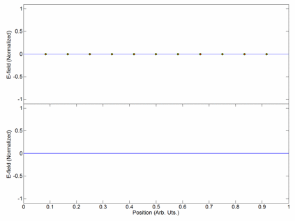
A mode-locked, fully reflecting cavity supporting the first 30 modes. The upper plot shows the first 8 modes inside the cavity (lines) and the total electric field at various positions inside the cavity (points). The lower plot shows the total electric field inside the cavity. |
Mode-locking is
a technique in optics by
which a laser can
be made to produce pulses of light of extremely short duration, on the order of picoseconds (10−12 s)
or femtoseconds (10−15 s).
A laser operated in this way is sometimes referred to as a femtosecond laser,
for example in modern refractive surgery.
The basis of the technique is to induce a fixed-phase relationship
between the longitudinal modes of
the laser's resonant cavity. Constructive
interference between
these modes can cause the laser light to be produced as a train of pulses. The laser is then said to be 'phase-locked' or 'mode-locked'. |

Laser scanning module with two galvanometers, from Scanlab AG. The red arrow shows the path of the laser beam. |
Laser scanning is
the controlled deflection of laser beams,
visible or invisible. Scanned
laser beams are used in some 3-D printers,
in rapid prototyping,
in machines for material processing, in laser engraving machines,
in ophthalmological laser systems for the treatment of presbyopia,
in confocal microscopy,
in laser printers,
in laser shows,
in Laser TV,
and in barcode scanners
Galvanometers (also
called "scanners" or "galvos") are computer-controlled electromagnetic devices that move mirrors mounted on the end of rotary shafts. The mirror reflects the laser beam to "draw" images. Galvanometers are typically identified by their speed of operation, measured in Kpps (kilo points per second). Available speeds include 8k, 12k, 20k, 30k, 35k, 50k, and 60k. The faster the galvanometers, the smoother and more flicker-free the projected image. Each galvanometer moves the beam in one plane, either X axis or Y axis. Placing the galvanometers close together at 90 degrees to each other allows full movement of the laser beam within a defined square area. The most useful specifications of a galvanometer pair for laser show use are the speed at which they can draw points, and the angle at which they achieve this speed. Galvanometers come in two main groups: open
loop and closed
loop. Closed loop, which is most common, means the galvanometer is controlled by a servo system—the
control circuit uses a feedback signal
generated by the mirror's motion to correct motion commands. An amplifier similar
to an audio power
amplifier drives the mirror. |

For an ellipse, the aspect ratio denotes the ratio of the major
axis to
the minor axis.
An ellipse with an aspect ratio of 1:1 is a circle. |
The aspect ratio of a geometric shape is the ratio of its sizes in different dimensions. For example, the aspect ratio of a rectangle is the ratio of its longer side to its shorter side – the ratio of width to height, when
the rectangle is oriented as a "landscape".
The aspect ratio is most often expressed as two integer numbers separated by a colon (x:y), less commonly as a simple or decimal fraction. The values x and y do not represent actual widths and heights but, rather, the proportion between width and height. As an
example, 8:5, 16:10, 1.6:1, 8⁄5 and 1.6 are all ways of representing the same aspect ratio.
In objects of more than two dimensions, such as hyperrectangles, the aspect ratio can still be defined as the ratio of the longest side to the shortest side.
|

The basic symbol of surface roughness |
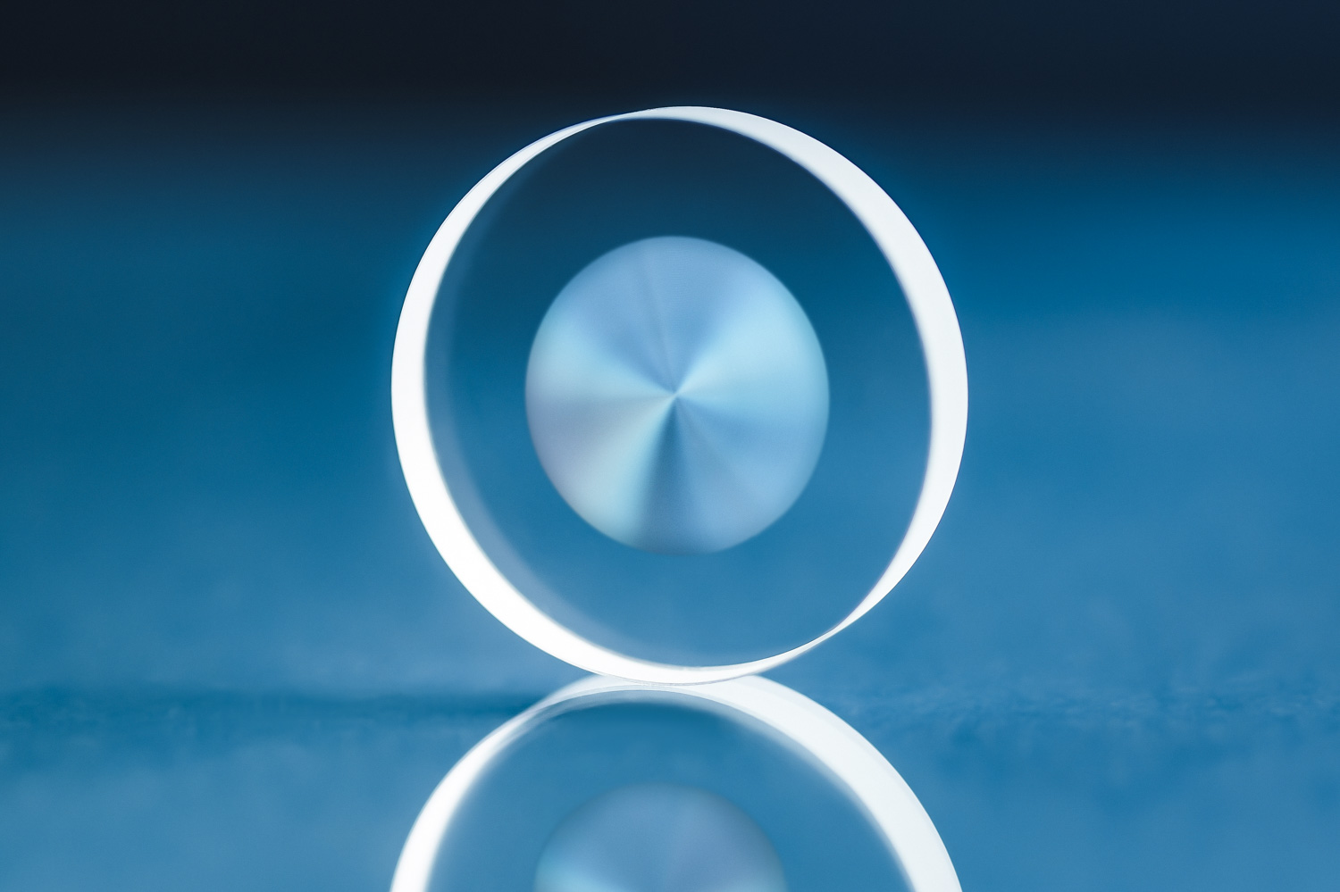
Surface roughness, often shortened to roughness, is a component of surface texture. It is quantified by the deviations in the direction of the normal vector of a real surface from its ideal form. If these deviations are large, the surface is rough; if they are small, the surface is smooth. In surface metrology, roughness is
typically considered to be the high-frequency, short-wavelength component of a measured surface. However, in practice it is often necessary to know both the amplitude and frequency to ensure that a surface is fit for a purpose.
Roughness plays an important role in determining how a real object will interact with its environment. In tribology, rough surfaces usually wear more quickly and have higher friction coefficients than smooth surfaces. Roughness is often a good predictor of the performance of a mechanical component, since irregularities on the surface may form nucleation sites for cracks or corrosion. On the other hand, roughness may promote adhesion.
|

Laser marked electronic part |
Laser engraving is the practice of using lasers to engrave an object. Laser marking, on the other hand, is a broader category of methods to leave marks on an object, which also includes color change due to chemical/molecular alteration, charring, foaming, melting, ablation, and more. The technique does not involve the use of inks, nor does it involve tool
bits which contact the engraving surface and wear out, giving it an advantage over alternative engraving or marking technologies where inks or bit heads have to be replaced regularly.
The impact of laser marking has been more pronounced for specially designed "laserable" materials and also for some paints. These include laser-sensitive polymers and novel metal alloys.
The term laser marking is also used as a generic term covering a broad spectrum of surfacing techniques including printing, hot-branding and laser bonding. The machines for laser engraving and laser marking are the same, so that the two terms are sometimes confused by those without knowledge or experience in the practice.
|
Glass to metal welding |
Laser beam welding (LBW)
is a welding technique
used to join pieces of metal or thermoplastics through the use of a laser.
The beam provides a concentrated heat source, allowing for narrow, deep welds and high welding rates. The process is frequently used in high volume applications using automation,
as in the automotive industry. It is based on keyhole or penetration mode welding. |
Waveguide writing |
An optical waveguide is a physical structure that guides electromagnetic waves in the optical spectrum. Common types of optical waveguides include optical
fiber and transparent dielectric waveguides made of plastic and glass.
Optical waveguides are used as components in integrated optical circuits or as the transmission medium in local and long haul optical communication systems.
Optical waveguides can be classified according to their geometry (planar, strip, or fiber waveguides), mode structure (single-mode, multi-mode), refractive index distribution (step or gradient index) and material (glass, polymer, semiconductor).
|
Multiphoton polymerization | MPP
: Superconducting coil on silicon wafer |
Multiphoton lithography (also known as direct laser lithography or direct laser writing) of polymer templates has been known for years[timeframe?] by
the photonic crystal community. Similar to standard photolithography techniques, structuring is accomplished by illuminating negative-tone or positive-tone photoresists via light of a well-defined wavelength. The fundamental difference is, however, the avoidance of reticles. Instead, two-photon
absorption is utilized to induce a dramatic change in the solubility of the resist for appropriate developers.
Hence, multiphoton lithography is a technique for creating small features in a photosensitive material, without the use of complex optical systems or photomasks. This method relies on a multi-photon absorption process in a material that is transparent at the wavelength of the laser used for creating the
pattern. By scanning and properly modulating the laser, a chemical change (usually polymerization) occurs at the focal spot of the laser and can be controlled to create an arbitrary three-dimensional periodic or non-periodic pattern. This method has been used for rapid prototyping of structures with fine features.
|

Other names
IUPAC name
poly(dimethylsiloxane)
PDMS
dimethicone
dimethylpolysiloxane
E900
|
Polydimethylsiloxane (PDMS), also known as dimethylpolysiloxane or dimethicone, belongs to a group of polymeric organosilicon compounds that are commonly referred to as silicones.PDMS
is the most widely used silicon-based organic polymer, as its versatility and properties lead to many applications.
It is particularly known for its unusual rheological (or flow) properties. PDMS is optically clear and, in general, inert, non-toxic, and non-flammable. It is one of several types of silicone oil (polymerized siloxane).
Its applications range from contact lenses and medical devices to elastomers; it is also present in shampoos (as it makes hair shiny and slippery), food (antifoaming agent), caulking, lubricants and heat-resistant tiles.
|
II. Microfluidic Chips and Devices Manufacturing
Microelectromechanical systems chip, sometimes called "lab on a chip"
|
A lab-on-a-chip (LOC)
is a device that integrates one or several laboratory functions
on a single integrated circuit (commonly
called a "chip") of only millimeters to a few square centimeters to achieve automation and high-throughput screening.LOCs
can handle extremely small fluid volumes down to less than pico-liters.
Lab-on-a-chip devices are a subset of microelectromechanical systems (MEMS)
devices and sometimes called "micro total analysis systems" (µTAS). LOCs may use microfluidics,
the physics, manipulation and study of minute amounts of fluids. However, strictly regarded "lab-on-a-chip" indicates generally the scaling of single or multiple lab processes down to chip-format, whereas "µTAS" is dedicated to the integration of the total sequence of lab processes to perform chemical analysis. The term "lab-on-a-chip" was introduced when it turned out that µTAS technologies were applicable for more than only analysis purposes. |

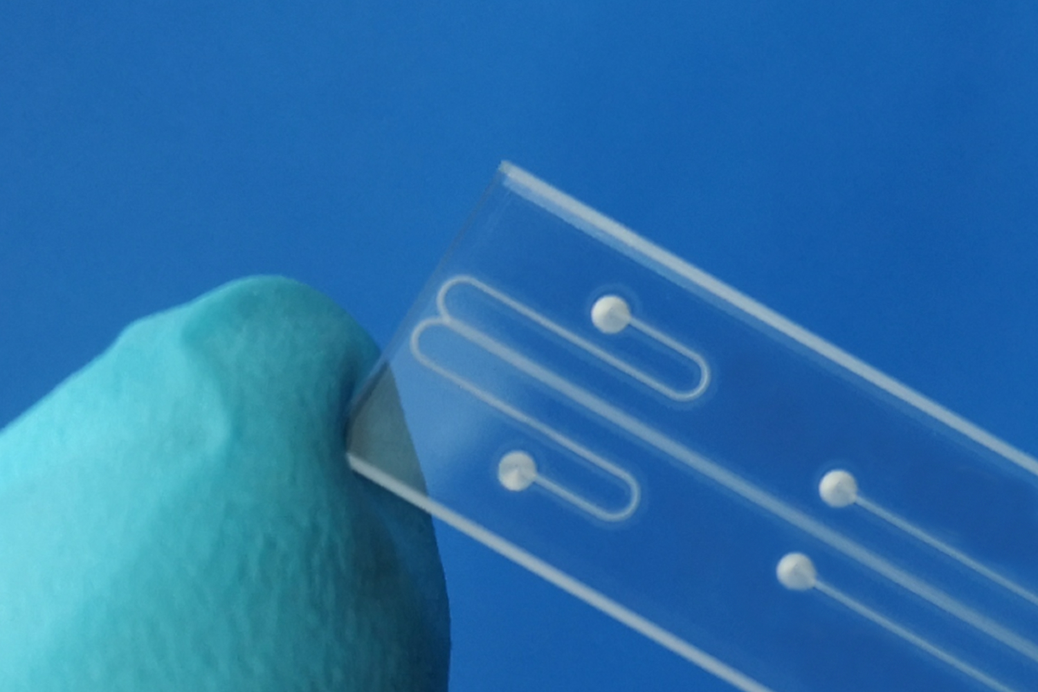
Silicone rubber and glass microfluidic devices. Top: a photograph of the devices. Bottom: Phase
contrast micrographs of
a serpentine channel ~15 μm wide.
|
Microfluidics refers
to the behavior, precise control, and manipulation of fluids that
are geometrically constrained to a small scale (typically sub-millimeter) at which surface forces dominate volumetric forces. It is a multidisciplinary field that involves engineering, physics, chemistry, biochemistry, nanotechnology,
and biotechnology.
It has practical applications in the design of systems that process low volumes of fluids to achieve multiplexing,
automation, and high-throughput screening.
Microfluidics emerged in the beginning of the 1980s and is used in the development of inkjet printheads, DNA
chips, lab-on-a-chip technology,
micro-propulsion, and micro-thermal technologies. |

Microtiter plates with 96, 384 and 1536 wells
|
A microplate or microtiter plate (Microtiter is a registered trademark in the United States therefore should not be used generically, attribution must be given), microwell plate, multiwell, is a flat plate with multiple "wells" used as small test tubes. The microplate has become a standard tool in analytical research and clinical diagnostic testing laboratories. A very common usage is in the enzyme-linked
immunosorbent assay (ELISA), the basis of most modern medical diagnostic testing in humans and animals.
A microplate typically has 6, 12, 24, 48, 96, 384 or 1536 sample wells arranged in a 2:3 rectangular matrix. Some microplates have been manufactured with 3456 or 9600 wells, and an "array tape" product has been developed that provides a continuous strip of microplates embossed on a flexible plastic tape.
|

|
Point-of-care testing (POCT or bedside
testing) is defined as medical diagnostic
testing at
or near the point of care—that
is, at the time and place of patient care. This
contrasts with the historical pattern in which testing was wholly or mostly confined to the medical laboratory,
which entailed sending off specimens away
from the point of care and then waiting hours or days to learn the results, during which time care must continue without the desired information. |

This single cell shows the process of the central
dogma of molecular biology, which are all steps researchers are interested to quantify (DNA, RNA, and Protein). |
In the field of cellular
biology, single-cell
analysis is the study of genomics, transcriptomics, proteomics, metabolomics and cell–cell
interactions at
the single cell level. Due
to the heterogeneity seen in both eukaryotic and prokaryotic cell populations, analyzing a single cell makes it possible to discover mechanisms not seen when studying a bulk population of cells. Technologies
such as fluorescence-activated cell sorting (FACS)
allow the precise isolation of selected single cells from complex samples, while high throughput single cell partitioning technologies, enable
the simultaneous molecular analysis of hundreds or thousands of single unsorted cells; this is particularly useful for the analysis of transcriptome variation in genotypically identical cells, allowing the definition of otherwise undetectable cell subtypes. The development of new technologies is increasing our ability to analyze the genome and transcriptome of single cells, as
well as to quantify their proteome and metabolome. Mass
spectrometry techniques have become important analytical tools for proteomic and metabolomic analysis of single cells. Recent
advances have enabled quantifying thousands of protein across hundreds of single cells,and
thus make possible new types of analysis. In
situ sequencing and fluorescence in situ hybridization (FISH)
do not require that cells be isolated and are increasingly being used for analysis of tissues. |
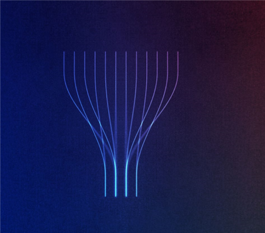
Diagram of flow focusing droplet formation device commonly used in microfluidic devices. Liquid flowing in from the left is pinched off into droplets by an oil flowing in from the top and bottom. |
Droplet-based microfluidics manipulate
discrete volumes of fluids in immiscible phases with low
Reynolds number and laminar
flow regimes. Interest
in droplet-based microfluidics systems has been growing substantially in past decades.Microdroplets
offer the feasibility of handling miniature volumes (μl to fl) of fluids conveniently, provide better mixing, encapsulation, sorting, sensing and are suitable for high throughput experiments.Two
immiscible phases used for the droplet based systems are referred to as the continuous phase (medium in which droplets flow) and dispersed phase (the droplet phase). |
III. Contract Manufacturing Services

Quartz sand (silica)
is the main raw material in commercial glass production
|
Glass is
a non-crystalline,
often transparent amorphous
solid, that has widespread practical, technological, and decorative use in, for example, window panes, tableware,
and optics.
Silicon dioxide (SiO2)
is a common fundamental constituent of glass. Fused quartz is
a glass made from chemically-pure silica.[65] It
has very low thermal expansion and excellent resistance to thermal shock,
being able to survive immersion in water while red hot, resists high temperatures (1000–1500 °C) and chemical weathering, and is very hard. It is also transparent to a wider spectral range than ordinary glass, extending from the visible further into both the UV and IR ranges,
and is sometimes used where transparency to these wavelengths is necessary. Fused quartz is used for high-temperature applications such as furnace tubes, lighting tubes, melting crucibles, etc.[69] However,
its high melting temperature (1723 °C) and viscosity make it difficult to work with. Therefore, normally, other substances (fluxes) are added to lower the melting temperature and simplify glass processing |

A vandalised telephone
booth with
tempered glass
|
Tempered or toughened glass is a type of safety glass processed by controlled thermal or chemical treatments to increase its strength compared with normal glass. Tempering puts the outer surfaces into compression and
the interior into tension. Such stresses cause the glass, when broken, to shatter into small granular chunks instead of splintering into jagged shards as ordinary annealed glass does. The granular chunks are less likely to cause injury.
Tempered glass is used for its safety and strength in a variety of applications, including passenger vehicle windows, shower doors, aquariums, architectural glass doors and tables, refrigerator trays, mobile phone screen protectors, bulletproof glass components, diving masks, and plates and cookware.
|

Samples of amorphous metal, with millimeter scale
|
An amorphous
metal (also
known as metallic glass or glassy
metal) is a solid metallic material,
usually an alloy,
with disordered atomic-scale structure. Most metals are crystalline in
their solid state, which means they have a highly ordered arrangement of atoms.
Amorphous metals are non-crystalline, and have a glass-like structure.
But unlike common glasses, such as window glass, which are typically electrical insulators,
amorphous metals have good electrical conductivity and
they also display superconductivity at
low temperatures. |
|
Ceramic materials may
have a crystalline or partly crystalline structure, with long-range order on atomic scale. Glass ceramics may have an amorphous or glassy structure, with limited or short-range atomic order. They are either formed from a molten mass that solidifies on cooling, formed and matured by the action of heat, or chemically synthesized at low temperatures using, for example, hydrothermal or sol-gel synthesis.
|
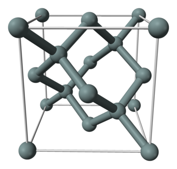
Silicon crystallizes in a diamond cubic
crystal structure by
forming sp3 hybrid
orbitals.
|
The late 20th century to early 21st century has been described as the Silicon Age (also known as the Digital
Age or Information
Age) because of the large impact that elemental silicon has on the modern world economy. The small portion of very highly purified elemental silicon used in semiconductor
electronics (<
10%[citation
needed])
is essential to the metal–oxide–semiconductor (MOS) transistors and integrated
circuit chips
used in most modern technology such as smartphones and
other computers.
The most widely used silicon device is the MOSFET (metal–oxide–semiconductor
field-effect transistor), which has been manufactured in larger numbers than any other device in history.
|

Single crystal sapphire boule grown by the Kyropoulos
method. Approximately 200 millimetres (8 in) in diameter, weighing approximately 30 kg (66 lb). (A second boule is visible in the background.)
|
Sapphire is
a precious gemstone,
a variety of the mineral corundum,
consisting of aluminium oxide (α-Al2O3)
with trace amounts of elements such as iron, titanium, chromium, vanadium,
or magnesium.
Commonly, natural sapphires are cut and polished into gemstones and worn in jewelry.
They also may be created synthetically in laboratories for industrial or decorative purposes in large crystal boules.
Because of the remarkable hardness of
sapphires – 9 on the Mohs scale (the
third hardest mineral, after diamond at
10 and moissanite at
9.5) – sapphires are also used in some non-ornamental applications, such as infrared optical components,
high-durability windows, wristwatch crystals
and movement bearings, and very thin electronic wafers,
which are used as the insulating substrates of
special-purpose solid-state electronics such
as integrated circuits and GaN-based
blue LEDs.
|

A roll of aluminium
foil
|
A foil is a very thin sheet of leaf, usually made by hammering or rolling. Foils are most easily made with malleable leaves, such as aluminium, copper, tin,
and gold. Foils usually bend under their own weight and can be torn easily. For example, aluminium foil is usually about 1/1000 inch (0.03 mm), whereas gold (more malleable than aluminium) can be made into foil only a few atoms thick, called gold
leaf. Extremely thin foil is called metal leaf. Leaf tears very easily and must be picked up with special brushes.
Foil is commonly used in household applications. It is also useful in survival situations, in the form of a "space blanket", where the reflective surface reduces the degree of hypothermia caused by thermal radiation.
|
Microfluidic Chips and Devices Manufacturing |
Engineering plastics are more robust and are used to make products such as vehicle parts, building and construction materials, and some machine parts. In some cases they are polymer blends formed by mixing different plastics together (ABS, HIPS etc). Engineering plastics can replace metals in vehicles, reducing their weight, with a 10% reduction improving fuel efficiency by 6-8%. Roughly 50% of the volume of modern cars is made of plastic but this only accounts for 12-17% of the vehicle weight.
High-performance plastics usually expensive, with their use limited to specialised applications which make use of their superior properties.
- Aramids: a class of heat-resistant and strong synthetic fibers used in aerospace and military applications, includes Kevlar and Nomex, and Twaron.
- Polyetheretherketone (PEEK): strong, chemical- and heat-resistant thermoplastic; its biocompatibility allows for use in medical implant applications and aerospace moldings. It is one of the most expensive commercial polymers.
- Polyetherimide (PEI) (Ultem): a high-temperature, chemically stable polymer that does not crystallize
- Polyimide: a high-temperature plastic used in materials such as Kapton tape
- Polysulfone: high-temperature melt-processable resin used in membranes, filtration media, water heater dip tubes and other high-temperature applications
- Polytetrafluoroethylene (PTFE), or Teflon: heat-resistant, low-friction coatings used in non-stick surfaces for frying pans, plumber's tape and water slides
- Polyamide-imide (PAI): High-performance engineering plastic extensively used in high performance gears, switches, transmission and other automotive components, and aerospace parts
|
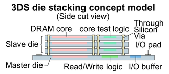
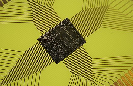
One master die and three slave dies
|
A three-dimensional
integrated circuit (3D
IC)
is a MOS (metal-oxide
semiconductor) integrated circuit (IC)
manufactured by stacking silicon wafers or dies and
interconnecting them vertically using, for instance, through-silicon vias (TSVs)
or Cu-Cu connections, so that they behave as a single device to achieve performance improvements at reduced power and smaller footprint than conventional two dimensional processes. The 3D IC is one of several 3D integration schemes that exploit the z-direction to achieve electrical performance benefits in microelectronics and nanoelectronics. |

A standard-sized 8-pin dual
in-line package (DIP)
containing a 555 IC.
|
Integrated circuits are
put into protective packages to
allow easy handling and assembly onto printed circuit boards and
to protect the devices from damage. A very large number of different types of package exist. Some package types have standardized dimensions and tolerances, and are registered with trade industry associations such as JEDEC and Pro
Electron. Other types are proprietary designations that may be made by only one or two manufacturers. Integrated
circuit packaging is
the last assembly process before testing and shipping devices to customers. |

BGA with an interposer between the integrated
circuit die to ball
grid array
|
An interposer is an electrical interface routing between one socket or connection to another. The purpose of an interposer is to spread a connection to a wider pitch or to reroute a connection to a different connection.
Interposer comes from the Latin word "interpōnere", meaning "to put between". They are often used in BGA packages, multi-chip modules and High Bandwidth Memory.
A common example of an interposer is an integrated circuit die to BGA, such as in the Pentium II. This is done through various substrates, both rigid and flexible, most commonly FR4 for rigid, and polyimide for
flexible. Silicon and glass are also evaluated as an integration method.Interposer
stacks are also a widely accepted, cost-effective alternative to 3D ICs. There are already several products with
interposer technology in the market, notably the AMD Fiji/Fury GPU,and the Xilinx Virtex-7 FPGA. In
2016, CEA Leti demonstrated their second generation 3D-NoC technology which combines small dies ("chiplets"), fabricated at the FDSOI 28 nm node, on a 65 nm CMOS interposer.
|

|
A probe card is an interface between an electronic test system and a semiconductor wafer. Typically the probe card is mechanically docked to a prober and electrically connected to a tester.
Its purpose is to provide an electrical path between the test system and the circuits on the wafer, thereby permitting the testing and validation of the circuits at the wafer level, usually before they are diced and packaged. It consists, normally, of a printed circuit board (PCB) and some form of contact elements, usually metallic, but possibly of other materials as well.
A semiconductor manufacturer will typically require a new probe card for each new device wafer and for device shrinks (when the manufacturer reduces the size of the device while keeping its functionality) because the probe card is effectively a custom connector that takes the universal pattern of a given tester and translates the signals to connect to electrical pads on the wafer. For testing of DRAM and FLASH memory devices these pads are typically made of aluminum and are 40–90 um per side. Other devices may have flat pads, or raised bumps or pillars made of copper, copper alloys or many types of solders
such as lead-tin, tin-silver and others.
|
|
Guide Plates for Probe Cards
Ceramic Plates and Glass Plates for the probe cards industry – an essential component for guiding probes for microchip inspection at the correct position. Fast prototyping and production services from 1 unit for your individual designs. The semiconductor industry further minimizing contact sizes and increasing density requires novel solutions to meet today’s market needs. While conventional processing methods cannot keep up with feature size minimization at the same quality level, industry-leading processing technology and experience ensure: Ultra-high precision & quality, Fast prototyping, Heat and force resistance, Small feature sizes, Diverse materials: ceramic (silicon carbide, silicon nitride) and many types of glasses and High aspect ratios unachievable with alternative technologies |

Sketch of the eWLB
package, the first commercialized FO-WLP technology
|
Fan-out wafer-level packaging (also known as wafer-level fan-out packaging, fan-out WLP, FOWL packaging, FO-WLP, FOWLP, etc.) is an integrated circuit packaging technology, and an enhancement of standard wafer-level packaging (WLP) solutions.
In conventional technologies, a wafer is diced first, and then individual dies are packaged; package size is usually considerably larger than the die size. By contrast, in standard WLP flows integrated circuits are packaged while still part
of the wafer, and the wafer (with outer layers of packaging already attached) is diced afterwards; the resulting package is practically of the same size as the die itself. However, the advantage of having a small package comes with a downside of limiting the number of external contacts that can be accommodated in the limited package footprint; this may become a significant limitation when complex semiconductor devices requiring a large number of contacts are considered.
Fan-out WLP was developed to relax that limitation. It provides a smaller package footprint along with improved thermal and electrical performance compared to conventional packages, and allows having higher number of contacts without increasing the die size.
In contrast to standard WLP flows, in fan-out WLP the wafer is diced first. But then the dies are very precisely re-positioned on a carrier wafer or panel, with space for fan-out kept around each die. The carrier is then reconstituted by molding, followed by making redistribution layer atop the entire molded area (both atop the chip and atop the adjacent fan-out area), and then forming solder
balls on top.
|

Intel 80186 in
QFJ68 / PLCC68, an example of a plastic leaded chip carrier
|
In electronics,
a chip carrier is
one of several kinds of surface-mount technology packages for integrated
circuits (commonly
called "chips"). Connections are made on all four edges of a square package; compared to the internal cavity for mounting the integrated circuit, the package overall size is large.Chip carriers may have either J-shaped metal leads for connections by solder or by a socket, or may be lead-less with metal pads for connections. If the leads extend beyond the package, the preferred description is "flat
pack".[1] Chip
carriers can be smaller than dual in-line packages and
since they use all four edges of the package they can have a larger pin count. Chip carriers may be made of ceramic or plastic. Some forms of chip carrier package are standardized in dimensions and registered with trade industry associations such as JEDEC.
Other forms are proprietary to one or two manufacturers. Sometimes the term "chip carrier" is used to refer generically to any package for an integrated circuit. |
IV.
Optical fibers

A bundle of optical fibers
|
Optical fibers typically include a core surrounded
by a transparent cladding material
with a lower index of refraction.
Light is kept in the core by the phenomenon of total internal reflection which
causes the fiber to act as a waveguide. Fibers
that support many propagation paths or transverse modes are
called multi-mode fibers,
while those that support a single mode are called single-mode fibers (SMF).Multi-mode
fibers generally have a wider core diameter and
are used for short-distance communication links and for applications where high power must be transmitted. Single-mode
fibers are used for most communication links longer than 1,000 meters (3,300 ft). |

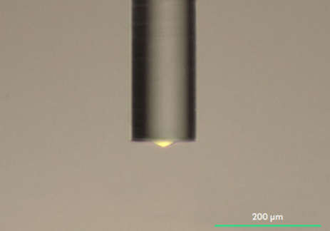
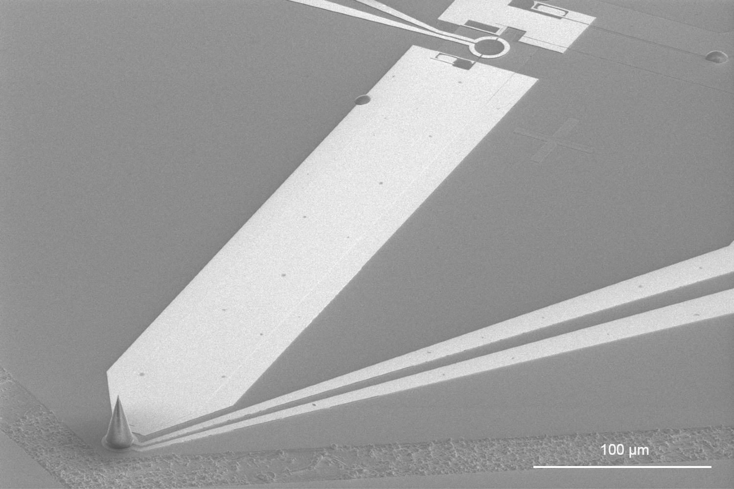
Optical fiber drilling
Optical fiber lens
|
Fibers Drilling / Tip Shaping
Laser drilling of optical fibers using femtosecond laser radiation is a state-of-the-art technique showing many advantages over conventional laser processing, mechanical drilling that enable precise process control.Features: No melting and micro-cracks in peripheries, Hole diameter as small as 10 μm, Precise control of taper angle and depth, Variable geometry of holes, Different processing parameters might be developed upon request.Tip Shaps : Lens (convex, concave, spherical ball) • Taper (up or down) • Diffuser • Side-fire • Angled end.
References :
Cold atoms in micromachined waveguides: A new platform for atom-photon interactionsProspects for strongly coupled atom-photon quantum nodes
|

A Fiber Bragg Grating structure, with refractive index profile and spectral response
|
A fiber
Bragg grating (FBG)
is a type of distributed Bragg reflector constructed
in a short segment of optical fiber that
reflects particular wavelengths of
light and transmits all others. This is achieved by creating a periodic variation in the refractive index of
the fiber core, which generates a wavelength-specific dielectric mirror.
Hence a fiber Bragg grating can be used as an inline optical fiber to
block certain wavelengths or it can be used as wavelength-specific reflector. |
V. Space Variant Retarders / Waveplate / Wave retarder

|
A waveplate or retarder is
an optical device
that alters the polarization state
of a light wave
travelling through it. Two common types of waveplates are the half-wave plate,
which shifts the polarization direction of linearly polarized light,
and the quarter-wave plate,
which converts linearly polarized light into circularly polarized light
and vice versa.A quarter-wave plate can be used to produce elliptical polarization as well. |

|
Polarization (also polarisation)
is a property applying to transverse waves that
specifies the geometrical orientation of the oscillations.In
a transverse wave, the direction of the oscillation is perpendicular to the direction of motion of the wave. |
S-waveplate converts linear polarization to radial or azimuthal polarization and circular polarization to n optical vortex.
|
The s polarization refers to polarization of a wave's electric field normal to
the plane of incidence (the z direction
in the derivation below); then the magnetic field is in the
plane of incidence. The p polarization refers to polarization of the electric field in the
plane of incidence (the xy plane
in the derivation below); then the magnetic field is normal to
the plane of incidence. |

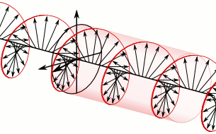
Azimuthal (upper) and Radial (lower) polarised laser beams
|
A beam of light has radial
polarization if
at every position in the beam the polarization (electric
field) vector points towards the centre of the beam. In practice, an array of waveplates may
be used to provide an approximation to a radially polarized beam. In this case the beam is divided into segments (eight, for example), and the average polarization vector of each segment is directed towards the beam centre.
An azimuth (;
from Arabic: اَلسُّمُوت, romanized: as-sumūt, lit. 'the
directions')[1] is
an angular measurement in
a spherical coordinate system. The vector from
an observer (origin) to a point of interest is projected perpendicularly onto
a reference plane;
the angle between the projected vector and a reference vector on the reference plane is called the azimuth. |
The electric
field vectors
of a traveling circularly polarized electromagnetic wave. This wave is right-circularly-polarized, since the direction of rotation of the vector is related by the right-hand rule to
the direction the wave is moving; or left-circularly-polarized according to alternative convention.
|
In electrodynamics, circular
polarization of
an electromagnetic wave is
a polarization state
in which, at each point, the electromagnetic field of
the wave has a constant magnitude and is rotating at a constant rate in a plane perpendicular to the direction of the wave. |

Diagram of different modes, four of which are optical vortices. Columns show the helical structures, phase-front and intensity of the beams
|
An optical
vortex (also
known as a photonic quantum vortex, screw
dislocation or phase
singularity) is a zero of an optical
field; a point of zero intensity.
The term is also used to describe a beam of light that has such a zero in it. The study of these phenomena is known as singular optics
Applications :
vortex coronagraph ,
optical tweezers spectral efficiency, orbital angular momentum based multiplexing, Quantum computing, cryptography, Stimulated Emission Depletion (STED) Microscopy,
polariton fluids, quantum vortices
|

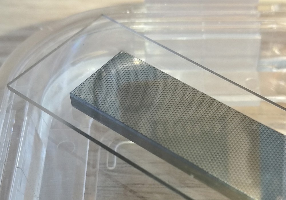
3D Laser Micro Milling for Polymer, Ceramic & Metal | IPG
|
Laser micromachining (also laser
beam micro-machining) means laser
machining of
very fine structures, typically on a scale between a few microns and a few hundred microns. The machined parts are not always very small, but at least the structures (e.g. holes, grooves or patterns) made on them. A micrometer-scale precision is required (e.g. for fine-cut contours with low roughness, and small heat-affected zones), thus the related term precision laser machining.
However, precision machining is not always part of micromachining. |

The Optical Cell Rotator is a fiber based laser trap that can hold and precisely orient living cells for tomographic microscopy.
|
Optical tweezers (originally called single-beam gradient force trap) are scientific instruments that use a highly focused laser beam to hold and move microscopic and sub-microscopic objects like atoms, nanoparticles and droplets, in a manner similar to tweezers.
If the object is held in air or vacuum without additional support, it can be called optical levitation.
The laser light provides an attractive or repulsive force (typically on the order of piconewtons), depending on the relative refractive index between particle and surrounding medium. Levitation is possible if the force of the light counters the force
of gravity. The trapped particles are usually micron-sized, or smaller. Dielectric and absorbing particles can be trapped, too.
Optical tweezers are used in biology and medicine (for example to grab and hold a single bacterium or cell like a sperm cell, blood
cell or DNA), nanoengineering and nanochemistry (to study and build materials from single molecules), quantum optics and quantum
optomechanics (to study the interaction of single particles with light). The development of optical tweezing by Arthur Ashkin was lauded with the 2018 Nobel Prize in Physics.
|
An electromagnetic (or any other) wave experiences partial transmittance and partial reflectance when the medium through which it travels suddenly changes. |
The transmission
coefficient is
used in physics and electrical
engineering when wave
propagation in
a medium containing discontinuities is
considered. A transmission coefficient describes the amplitude, intensity, or total power of a transmitted wave relative to an incident wave. |
|
|
|

Anti-reflective coatings are often used in camera lenses, giving lens elements distinctive colours. |
An antireflective or anti-reflection (AR) coating is
a type of optical coating applied
to the surface of lenses and
other optical elements to reduce reflection.
In typical imaging systems, this improves the efficiency since less light is
lost due to reflection. In complex systems such as telescopes and microscopes the
reduction in reflections also improves the contrast of
the image by elimination of stray light.
This is especially important in planetary astronomy.
In other applications, the primary benefit is the elimination of the reflection itself, such as a coating on eyeglass lenses
that makes the eyes of the wearer more visible to others, or a coating to reduce the glint from a covert viewer's binoculars or telescopic
sight. |

A plume ejected from a SrRuO3 target
during pulsed laser deposition. |
The laser
damage threshold (LDT) or laser
induced damage threshold (LIDT) is
the limit at which an optic or material will be damaged by a laser given
the fluence (energy
per area), intensity (power
per area), and wavelength.
LDT values are relevant to both transmissive and reflective optical elements and in applications where the laser induced modification or destruction of a material is the intended outcome. |

A packaged laser diode shown with a penny for
scale |
A laser diode (LD, also injection laser diode or ILD, or diode laser) is a semiconductor device similar to a light-emitting diode in which a diode pumped directly with electrical current can create lasing conditions at the diode's junction
Driven by voltage, the doped p–n-transition allows for recombination of an electron with a hole. Due to the drop of the electron from a higher energy level to a lower one, radiation, in the form of an emitted photon is generated. This is spontaneous emission. Stimulated emission can be produced when the process is continued and further generates light with the same phase, coherence and wavelength.
The choice of the semiconductor material determines the wavelength of the emitted beam, which in today's laser diodes range from infra-red to the UV spectrum. Laser diodes are the most common type of lasers produced, with a wide range of uses that include fiber optic communications, barcode readers, laser pointers, CD/DVD/Blu-ray disc
reading/recording, laser printing, laser scanning and light beam illumination. With the use of a phosphor like that found on white LEDs, Laser diodes can be used for general illumination.
|
Flat Axicon - Transforms Gaussian beam into a Bessel-Gauss beam |
An axicon is a specialized type of lens which has a conical surface. An axicon transforms a laser beam into a ring shaped distribution. They
can be convex or concave and be made of any optical material. The combination with other axicons or lenses allows a wide variety of beam patterns to be generated. It can be used to turn a Gaussian beam into a non-diffractive Bessel-like beam. Axicons were first proposed in 1954 by John McLeod.
Axicons are used in atomic traps and for generating plasma in wakefield accelerators. They
are used in eye surgery in cases where a ring-shaped spot is useful.
The Axicon is usually characterized by the ratio of the diameter of the ring to the distance from the lens tip to image plane d/l.
|

Intensity of a simulated Gaussian beam around focus at
an instant of time, showing two intensity
peaks for each wavefront. |
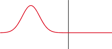
In optics,
a Gaussian beam is
a beam of electromagnetic
radiation with
high monochromaticity whose amplitude envelope in the transverse plane is given by a Gaussian function;
this also implies a Gaussian intensity (irradiance)
profile. This fundamental (or TEM00) transverse Gaussian
mode describes the intended output of most (but not all) lasers, as such a beam can be focused into the most concentrated spot. |

Evolution of a Bessel beam. |
A Bessel
beam is
a wave whose amplitude is described by a Bessel function of the first kind. Electromagnetic, acoustic, gravitational,
and matter waves
can all be in the form of Bessel beams. A true Bessel beam is non-diffractive. This means that as it propagates, it does not diffract and
spread out; this is in contrast to the usual behavior of light (or sound), which spreads out after being focused down to a small spot. Bessel beams are also self-healing,
meaning that the beam can be partially obstructed at one point, but will re-form at a point further down the beam axis. |
Flat-top intensity distribution after converter
|
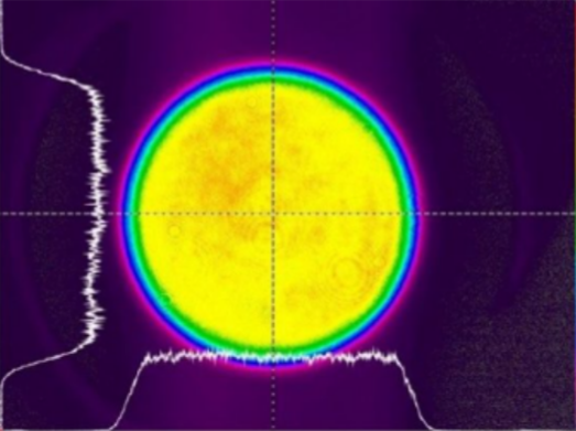
In optics,
a tophat (or top-hat) beam such
as a laser beam or
electron beam has a near-uniform fluence (energy
density) within a circular disk. It is typically formed by diffractive optical elements from
a Gaussian beam.
Tophat beams are often used in industry, for example for laser drilling of
holes in printed circuit boards.
They are also used in very high power laser systems, which use chains of optical amplifiers to
produce an intense beam. Tophat beams are named for their resemblance to the shape of a top hat. |

A laser beam profiler. |
A laser
beam profiler captures,
displays, and records the spatial intensity profile
of a laser beam at
a particular plane transverse to the beam propagation path. Since there are many types of lasers — ultraviolet, visible, infrared, continuous
wave, pulsed, high-power, low-power — there is an assortment of instrumentation for measuring laser beam profiles. No single laser beam profiler can handle every power level, pulse duration, repetition rate, wavelength,
and beam size. |

Compensates depolarization in the gain medium |
A depolarizer or depolariser is an optical device used to scramble the polarization of light. An ideal depolarizer would output randomly polarized light whatever its input, but all practical depolarizers produce pseudo-random output polarization.
Optical systems are often sensitive to the polarization of light reaching them (for example grating-based spectrometers). Unwanted polarization of the input to such a system may cause errors in the system's output.
|

Simplified scheme of levels a gain medium |
The active laser medium (also called gain medium or lasing medium) is the source of optical gain within a laser. The gain results from the stimulated emission of photons through electronic or molecular transitions to a lower energy state from a higher energy state previously populated by a pump
source.
Examples of active laser media include:
- Certain crystals, typically doped with rare-earth ions (e.g. neodymium, ytterbium, or erbium)
or transition metal ions (titanium or chromium); most often yttrium aluminium garnet (Y3Al5O12), yttrium
orthovanadate (YVO4), or sapphire (Al2O3);[1] and not often Caesium
cadmium bromide (CsCdBr3)
- Glasses, e.g. silicate or phosphate glasses, doped with laser-active ions;
- Gases, e.g. mixtures of helium and neon (HeNe), nitrogen, argon, carbon
monoxide, carbon dioxide, or metal vapors;
- Semiconductors, e.g. gallium arsenide (GaAs), indium gallium arsenide (InGaAs), or gallium nitride (GaN).
- Liquids, in the form of dye solutions as used in dye lasers
|
|